
Chen Liwu: Intel's goal is "10x in 5-10 years", betting on advanced packaging, glass substrates, and artificial diamonds

Intel CEO Patrick Gelsinger stated that his return goal for Intel is to "achieve a 10x return within 5 to 10 years" and is systematically reshaping Intel’s technology roadmap around advanced packaging, novel semiconductor materials, and next-generation substrate technologies.
In a recent podcast, Gelsinger elaborated on his path to transforming Intel: after strengthening the balance sheet and refocusing on the product line, he is now shifting the focus to advanced packaging technologies such as EMIB, glass substrates, and new materials like gallium nitride (GaN), silicon carbide (SiC), indium phosphide (InP), and synthetic diamonds, to tackle the challenges posed by traditional process nodes approaching their physical limits. He also revealed that the boom in AI agents and inference scenarios is driving robust demand for CPUs, with the CPU-to-GPU ratio in data center servers evolving from eight-to-one in the past to four-to-one or even lower.
Gelsinger noted that over the past 14 months, Intel shareholders have seen approximately a 6x return, but "this is just the beginning." He expects that by 2030 to 2032, the world will begin to truly recognize Intel’s potential—not just within the traditional PC client base, but also extending into edge computing, physical AI, and agent AI emerging markets.
In his view, if Intel’s XPU, advanced packaging, and foundry capabilities can be effectively integrated, they will provide customized chip solutions for different workloads—this is the long-term strategic direction he’s setting for the company.
New Materials as the Key Breakthrough, Focus on Advanced Packaging and Glass Substrates
With traditional process node scaling rapidly approaching physical limits, Gelsinger is pointing the breakthrough towards materials science and advanced packaging. He stated that Intel has already achieved mass production with its 18A process and is pushing towards 14A, being able to envision 10nm and even 7nm technical paths, but "this path will only get more expensive and more challenging."
To this end, Gelsinger has initiated multiple ventures in packaging materials. He invested in glass substrate company 3DGS, valuing the unique thermal and insulative properties of glass; for inter-chip connectivity, Intel is promoting the next-generation advanced packaging technology EMIB and has announced advanced packaging manufacturing collaborations in India and New Mexico, USA. Intel holds about 1,000 patents in the module space, and how to effectively integrate substrates and modules is a core engineering challenge that Gelsinger emphasizes.
In terms of new semiconductor materials, Gelsinger noted investments in GaN, SiC, and InP, some of which have already been acquired by major semiconductor companies such as ADI. He has also invested in a synthetic diamond wafer company, optimistic about the use of diamond as a thermal insulator in chip packaging. “That’s the engineer’s spirit—you’re constantly encountering bottlenecks, then find a way to leap over or bypass them,” he said.
Foundry Business: Trust Above All, Yield and Cycle Time as Core Metrics
Intel’s wafer foundry business was once seen as unsustainable by outsiders, yet Gelsinger chose to hold firm. He stated the core rationale behind this decision: advanced U.S. domestic manufacturing holds strategic value for supply chain security, and no major semiconductor enterprise can afford to concentrate their supply chain in just one or two geographical regions.
On execution, Gelsinger set yield, defect density, and cycle time as the top priorities for the foundry business. He emphasized that foundry is ultimately a business of trust—"Customers must trust you before handing you their wafers." Once yields fall short and customers lose revenue, it’s difficult to win them back.
He also revealed that Intel and TSMC are partners and not mere competitors; the industry as a whole needs more capacity to meet continuing demand growth. He expects that by 2030 to 2032, the true potential of Intel’s foundry business will start to be realized in the market.
Terafab Partnership: Building Semiconductor Infrastructure with Elon Musk
Gelsinger disclosed that the Terafab project with Elon Musk emerged from a shared realization—that semiconductor infrastructure development in capacity, production, and power efficiency is lagging far behind the growth in AI demand. Within this collaboration, Musk decided to build his own wafer fab, with Intel providing technology and process support to accelerate production. Gelsinger mentioned he meets weekly with Musk’s team, and the cooperation is progressing smoothly.
He also noted that Musk has unconventional ideas on the operational side, such as once discussing whether smoking could be allowed in certain cleanroom areas: "I might not go that far, but maybe certain areas are okay—the key is keeping an open mind."
The Biggest Misunderstanding Among Investors: Intel Is Still in the 'Crawling' Stage, True Potential Emerges After 2030
Facing doubts about Intel’s transformation progress, Gelsinger referenced his signature "crawl-walk-run" framework. He stated that the past few months were still at the "crawl" stage: in terms of building CPU, GPU, and software architecture teams, Intel is quietly laying the groundwork and striving to innovate at the speed of a large startup; on the foundry side, the gap with TSMC remains significant, so humility is required to solidify IP, yield, and other fundamental capabilities.
"My VC instinct tells me—to seek opportunities for 10x returns," Gelsinger said. Citing his experience at Cadence: from interim CEO to stepping down, he created about 76 to 85x returns for shareholders. He admitted, Intel is a much larger, harder-to-replicate company, but 'achieving 10x returns in 5 to 10 years' is the clear target I’ve set for myself.
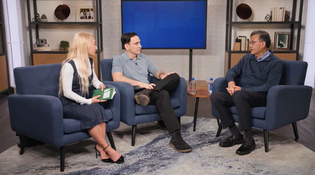
The following is a transcript of the interview:
Host: Welcome back to No Priors. Today, Allad and I are joined by Patrick Gelsinger—a legendary investor from Walden, former Cadence CEO, and now CEO of Intel. We’ll discuss his plans to transform Intel, what it means to have the U.S. government as a major shareholder, how to become a great semiconductor investor, and whether we can manufacture chips in the U.S. Welcome, Pat.
Why Take on the Intel Challenge?
Host: Let’s start with the obvious. Taking on the CEO role at this exceedingly important American semiconductor company is a truly tough job. Why did you accept?
Gelsinger: That’s a good question. I’m 66, and many have said I should retire, asking why take on the hottest job in the industry. A few reasons: One, it’s an iconic company, pivotal for the entire semiconductor ecosystem and America; two, after Cadence, I decided to do one more big thing.
Host: A lot has happened this past year. What surprised you the most?
Gelsinger: The biggest surprise was something I had never encountered in any previous job or training—a morning, President Trump asked me to resign, citing a conflict of interest, no exceptions. I first convinced myself: I don’t need this job, I’m doing this solely to save Intel. After setting aside emotions, I considered how I could help Intel. Fortunately, I got a meeting Thursday morning and again Monday. I presented my background: born in Malaysia, raised in Singapore, MIT grad, lived in the U.S. ever since—I shared this with him, he listened, and gave me a chance to stay. I’m very grateful for that.
Host: You described this job as "saving Intel." In your mind, what does it look like for Intel to win and thrive?
Gelsinger: It’s been 14 months and much has happened. First, it’s about driving a cultural shift, establishing accountability, and speeding up decision-making. I’m used to the pace of startups—everything moving at lightspeed—but Intel has layers upon layers of bureaucracy, and that must change. Second, is listening to customers—making them truly happy requires humility, a willingness to listen, and tackling their issues head-on. Third, from day one, I decided that all engineering teams report directly to me. Having an engineering background, I want to personally know where problems lie and what needs correcting. Listen to customers, make them happy, ensure we have the right products, streamline the portfolio, and set a clear roadmap and vision for the next five to ten years.
Intel’s Decadal Vision
Host: What’s your vision for Intel ten years down the road?
Gelsinger: My consistent approach—at Cadence or Intel—is to crawl first, remain humble, listen to customers; then walk; and finally, get up and run. Step by step.
The first move was to shore up the balance sheet—to be honest, it was in pretty bad shape at the time. I’m glad the U.S. government became a major shareholder. I explained to President Trump: Look at Japan, at Singapore—this is foundational infrastructure, and government support is natural.
Next, I’m deeply grateful for my old friend Jensen Huang—he invested $5 billion in Intel, and I’m pleased with the value we’ve created, as those $5 billion have grown to $25 billion or more. Also, Masayoshi Son from SoftBank—whom I served on their board—stepped in as well. Through these, we strengthened the balance sheet.
Afterwards, the focus turned to product—streamlining the portfolio, listening to customers, and rolling out the next-generation leading products. Now, agent AI and inference CPU demand is exceptional, so in a way, I came at the right time. The previous CPU-to-GPU ratio during training was about one to eight, but now I see it becoming one to four, even lower. CPUs are important again, which makes me happy.
I’ve talked to some AI model developers—they say, during reinforcement learning and scheduling agents, CPUs outperform. So, CPU demand for me is high. After establishing a solid base in the data center server product line, the other key business is our foundry. It’s capital intensive and not easy. You need the right IP portfolio—for example, low-power IP for mobile clients, without which you can’t serve them. This is a service industry, but also a trust business—if yield is subpar, customers drop out due to revenue loss. So I’m laser focused on yield, defect density, and cycle time, ensuring we deliver high-quality, highly reliable customer service. The endgame is a full stack, not just the silicon itself—you need software; customers directly ask me, "give me the whole rack," and you have to offer system-level solutions. I’m steadily pushing these steps, while recruiting the best talent I can find. By the way, I do all hiring personally, without headhunters.
Collaborating with Elon Musk on Terafab
Host: Another highly discussed move is Terafab and the collaboration with Elon Musk. Can you discuss how this came about and how you work together?
Gelsinger: I think we both agree, Elon Musk is one of the greatest entrepreneurs of this century. We both recognized that semiconductor infrastructure hasn’t kept pace with AI growth—in terms of capacity, production efficiency, or power efficiency. We both saw this gap.
Also, I enjoy working with him. He’s extremely unconventional, asking "why do it the traditional way" at every step, which is refreshing. I enjoy hearing disagreements, then together finding the optimal path. Both sides learn a lot. He has a clear vision—his robots and cars need a massive number of chips.
Specifically, Terafab is his decision to build his own wafer fab, and we’re happy to help him accelerate production using some of our technologies and processes—a collaborative project for both parties. His team is excellent. I meet with them every week. Collaborating with him is exhilarating. He’s suggested unconventional ideas, like smoking in cleanrooms—which I might not go that far with, maybe in certain areas it’s possible; the key is an open mind. We’re listening and assessing with care.
Global Semiconductor Supply Chain Shifts
Host: From a macro perspective, how do you see AI driving changes in the global semiconductor supply chain by country?
Gelsinger: The impact of AI on the entire landscape will surpass the internet, and be even more profound. AI first makes you more efficient—tasks once laborious can now be swiftly completed with the help of many agents. For semiconductor design, timing optimization and time-to-market are greatly improved, and costs can drop.
AI demand faces several bottlenecks: first, power constraints, as some countries simply lack enough electricity; second, helium’s impact, which many people overlook even though it’s significant for the semi industry; third, memory shortages—now the most urgent problem. Even if you expand now, new capacity takes years to come online; CPUs and GPUs are also in short supply, and prices are rising, pushing costs downstream to clients.
The companies most at risk are those that don’t embrace AI. AI can boost nearly all functional departments, so businesses should actively adopt AI and find better ways to leverage it, whether for prediction, design, or various workloads.
Host: The simplest argument against Terafab and Intel foundry competitiveness concerns labor costs and domestic manufacturing viability. What logic drove you to double down on foundry?
Gelsinger: When deciding whether to persist or exit foundry, there were many voices outside—saying it’s too expensive, not feasible. But my judgment: it’s essential for America and for the sector.
We all experienced supply chain challenges; any major semiconductor company must seriously consider supply chain, and own a robust and resilient one, not solely relying on one or two highly concentrated suppliers. More people will realize U.S. domestic manufacturing is vital.
Our most advanced processes, such as 18A—i.e., 1.4nm level—we’re already planning for 1nm and 0.7nm. Process nodes are shrinking, width thinner than hair, extremely complex, any misstep and it’s all for naught. Hence, manufacturing precision is increasingly a bottleneck.
We hold TSMC in high regard; we’re good partners, and the industry needs more capacity for customers. That’s why we grit our teeth and persist—long term, it’s key, and a place I can add value to the industry.
Physical Limits and Advanced Packaging
Host: There’s been talk for years about chip scaling hitting physical limits; lines are so narrow you can’t go further. When will we hit the wall?
Gelsinger: We’re at 18A, pushing toward 14A, and can see paths to 10nm and 7nm—it’s achievable, but increasingly expensive and difficult. That’s why we need partners, and tight collaboration with substrate and equipment suppliers to boost yield and performance.
Another key bottleneck emerging is advanced packaging. TSMC has CoWoS; we have EMIB, a next-gen solution. I must ensure it can meet yield requirements in mass production.
When traditional scaling hits bottlenecks, I revisit materials science for breakthroughs—GaN, SiC, InP, I’ve invested in all three. With packaging materials, my attention is on glass—an excellent thermal insulator, led to an investment in 3DGS. Intel’s module portfolio has around 1,000 patents. How to integrate substrates and modules is a key topic. We’ve also announced advanced packaging partnerships in India and New Mexico. Additionally, I’m exploring synthetic diamonds—another superb thermal insulator—with investments in a diamond wafer firm.
That’s the engineer’s mentality—constantly hitting bottlenecks, finding ways over or around them. Having gone deep across the whole semi lifecycle from EDA tools to design to manufacturing, I’m delighted to put this experience to use and contribute to the industry.
Host: So is it conceivable that process node convergence will flatten performance differences across foundries, creating some sort of asymptote?
Gelsinger: The essence of Moore’s Law is the doubling of transistor density, but power and costs might not halve in sync—you can double performance, but area and cost won’t drop the same. Unless you find new materials or design methods. That’s why I’m now recruiting talents in materials science—it’s become core to innovation in this field.
18 years ago, when I was still investing in semis, many top VCs were uninterested in the field. In partner meetings, after my pitch, half would leave, the rest asking "any software or services projects?"—and only one or two would stay sympathetically. Now, Jensen Huang’s NVIDIA is worth $5.3 trillion, Broadcom and TSMC are at $2 trillion each, and my friend Lisa Su’s AMD is close to $800 billion, Intel about $600 billion. Semis are hot again—foundational. 15-20 years ago, almost no VCs would coinvest with me, besides Samsung, ARM, and SoftBank. Now VCs are piling in—it’s gratifying.
The Challenges of Semiconductor Investing
Host: As both a veteran investor and operator, you’ve experienced difficulties in semi investing—capital intensity, unpredictable outcomes, deep workload understanding, high supplier switching risk, strong cyclicality… How do you view these risks, and what advice do you have for investing within this supply chain?
Gelsinger: VC and entrepreneurship are in my blood—I truly enjoy it. Not to flex, but for context: I have 159 IPOs, 126 M&A exits, including over 200 semi investments, 38% in the U.S.
My approach always starts with a core question: where’s the bottleneck, what problem are you solving? For example, I invested in Cradle Semiconductor because interconnect has become a bottleneck; I invested in Celestial AI, as photonic interconnect within clusters is increasingly key—Jensen Huang has invested in nearly all photonics-related companies, not by coincidence.
Design-wise, can AI and ML help lower complexity or improve quality? I believe there’s huge opportunity in EDA, with several startups digging in—it’s a gold mine. In materials, GaN, SiC, and InP are my targets, and some have been acquired by ADI. Power management—losses converting 40V to 1V are huge—is another niche I favor.
My framework: is the problem real, do customers truly struggle with it, who is the first target customer? I prefer hyperscalers—they have the capacity and will; if they like you, will spend millions over years, possibly offering guarantees; landing a large customer enables scaling.
Talent is also crucial—the U.S., Silicon Valley, Austin, and Israel are my main focus. Israel has revolutionary, hard-working entrepreneurs. Even during wartime, meetings continue—often, "there’s an alert, I’ll go to the basement, maybe just audio,"—the resilience impresses me.
Now, besides agent AI, physical AI is the next major frontier—look at the full-stack; that’s why I’m still deeply involved in cutting-edge model investments—I see great promise in open source innovation for physical AI, it’s a gold mine.
Experience from Cadence
Host: You mentioned that AI brings faster, cheaper, more creative chip design and testing. Based on your Cadence experience, what areas hold the most potential, and have you seen any impact yet?
Gelsinger: After nearly 15 years at Cadence, one of my proudest accomplishments was finding and nurturing my successor—he’s an outstanding CEO, wholeheartedly embracing AI and integrating agent AI into tools to boost efficiency. Synopsys’ Sassine is doing the same, supported by a $2 billion NVIDIA investment, and acquiring Ansys for full-system design expansion.
The big firms are working on this, but there’s room for startups to do even more disruptive things, and eventually IPO or be acquired by the big two. It depends on the founder’s vision. My philosophy: if they want a quick exit, help them; if they aim for IPO from day one, help them pursue that. As VCs, we support founders’ dreams and help them realize them.
Scaling and Investment Decisions
Host: For the directions you mentioned—materials companies, EDA, manufacturing—if we look a decade out, will Intel or the next semiconductor company be transformed by AI?
Gelsinger: I think so. Returning to your points about capital intensity, unpredictability, and cyclicality—all need to be built into investment decisions. I like to enter early and build teams; find the right investors who stick with you through tough times, not just in good; and seek strategic backers, whether in manufacturing, memory, interconnect, or other value-added dimensions. I have some growth and hedge fund friends, with unique public market insights, who can advise founders on what directions to avoid—very useful.
Honestly, in reviewing my investments, 9 out of 10 companies pivoted their business plans midcourse as markets changed. I value team-based entrepreneurs, not solo. Also, an open mind, willingness to listen, absorb advice, but ultimately develop independent judgment—the best outcome isn’t "I do whatever I’m told," but that you provide enough feedback for them to independently conclude what you’d recommend. That’s the fun of entrepreneurship.
A decade from now, the winners will be those focusing on a niche, finding the right partners, and scaling. You need a full-stack solution, that’s important. The big firms can focus on the platform, like Jensen Huang did with CUDA, transforming NVIDIA into a platform company. Startups can move at lightspeed, like Anthropic or OpenAI, changing the game in their own ways and becoming leaders.
For Intel, I hope it can play this role—we have XPU, advanced packaging, foundry, and if we integrate these to customize chips for different workloads, that’s the path I’m headed towards.
Team Restructuring for the AI Era
Host: The software industry is changing dramatically—what kind of people to hire, who’s fit to manage multiple agents. Today there’s a tendency to hire people in their 30s to 50s, as they’re used to leading teams and this skill transfers to managing AIs. In hardware or a foundry context, how do you see the evolution of team structure and capabilities?
Gelsinger: Return to the crawl-walk-run framework. While crawling, I hired the best talents in semis. Now I’m considering what software talent is needed to build up a full stack; I also noticed the average team age is 40s to 50s—I need to bring in more young talent, people who understand workloads and cutting-edge open-source models.
Interestingly, my son has become my teacher. Every time I visit him and see my grandkids, I ask him about AI and ML—he knows more than me. I’ve learned a lot, then convert that knowledge into investment decisions and recruiting.
Intel used to be a very old-school, spreadsheet-dependent firm; I’m transitioning it to an AI-powered enterprise—not just in design, but to fully embrace AI everywhere, reducing spreadsheet reliance. Senior technical employees and AI tools must combine, not only in sales and marketing, but now design is rapidly embracing AI too.
Industrial Policy and Capital Sources
Host: For capital-intensive firms, financing is always a concern. Industrial policy has created giants like TSMC, but this approach is rarely embraced long-term in U.S. business culture. What’s your view?
Gelsinger: For capital-intensive and infrastructure projects, access to funds is critical. Now some VCs are willing to invest a billion dollars in a single company—that was unheard of before. So, for early strategy, get in very early while valuations are reasonable; or reach Series A, but A rounds are already over a billion, which is tough.
Growth capital sources, like mutual funds—not as sensitive to equity percentages—are welcome. For capital-intensive initiatives like AI plants or foundries, you have to seek government, sovereign wealth, or major infrastructure fund backing. Government and sovereign capital will be increasingly important.
As a listed company, I intentionally focus more on long-term growth-oriented investors and not those asking every quarter about buybacks—of course, shareholder value is important, but I have to build the business. The balance is crucial.
The Biggest Misunderstanding Investors Have About Intel
Host: What do you think is investors’ biggest misconception about Intel?
Gelsinger: Several things. Return to crawl-walk-run: we’re still crawling these past months, but the potential is starting to be seen. On products, in PC clients we still have market share, but performance needs big improvement—so I’m quietly building CPU, GPU, and software architecture teams to leap ahead, moving fast like a big startup, using better technologies to leapfrog.
On foundry, we still have a long way to go versus TSMC, and must remain humble and focus on foundations—IP, yield, defect density, cycle time—to make foundry more efficient and reliable. It’s a trust business—customers must trust you before handing over their wafers. These things take longer, but by 2030 to 2032, I believe people will start to see how big Intel’s real potential is.
PC client is our base, but we’re extending to the edge, to physical and agent AI. In the past, you just provided servers and PCs for humans, but now there’s another dimension—millions of agents needing compute, needing software stacks. I think both agent and physical AI are opportunities for Intel, the game isn’t over yet.
AI is just getting started—you have Jensen Huang dominating training, the edge, agent AI, and physical AI—it’s a huge opportunity, and everyone still has a shot. That’s the path I’m going all-in on. In the past 14 months, we’ve delivered 6x returns for shareholders, but this is just the start—there’s much more ahead.
My VC instincts say—find those 10x return opportunities. At Cadence, I was interim CEO to retirement, the stock went from $2.4 to a 76x return for shareholders; as executive chairman, around 85x. Intel is much larger and harder to replicate, but my goal is 10x—a 10x return in 5 to 10 years, that’s the VC in me.
Where Will Compute Power Reside?
Host: There’s a view that data centers will get ever larger, gigawatt is just the beginning, centralization is the mainstream. But your business blueprint seems to include edge and client compute. Do you think compute will ultimately be distributed across data centers, edge, clients, or driven entirely by application workload?
Gelsinger: Today’s large-scale AI infra build-out is right—I see no reason for slowdown, as workloads keep growing. The limiting factors are all supply side—any slowdowns stem from supply, not demand.
What I’m most focused on is: after all this infra is built, what applications will run on it? You need true scale apps—just like in the internet era, Amazon and Netflix stood out and others faded or got acquired. The AI industry will go through the same—after rapid growth, comes consolidation, and in the end, one or two true winners emerge.
Focusing on applications is key—Netflix is a real app, Amazon is a real app, and they won. Some use cases are more suitable for the edge or client—robotics, defense—there, device compute choices are critical. Your assumptions for connectivity and embedded capability determine what you can do—that was overlooked in the SaaS era.
My investment approach: find real problems, identify the right partner, assess whether app market size is sustainable—if you truly believe, double or triple down. Of course, that includes betting on apps that aren’t yet at scale.
Host: Thank you very much for joining us today—it’s been a real pleasure.
Gelsinger: Thanks for the invitation.
Disclaimer: The content of this article solely reflects the author's opinion and does not represent the platform in any capacity. This article is not intended to serve as a reference for making investment decisions.
You may also like
Singularity Future Technology Ltd stock sinks to $3.48, tests $2.86 support
Bitcoin Rewarded 1 of 2 US Interventions. Bessent Just Promised More
XRP breaks consolidation, whales add 190 million coins amid 22% weekly surge
Arbitrum RWA holders cross 10K – Can ARB extend its 16% rally?
Crypto prices
More


